NDC International is pleased to announce that we are partnering with ESTEK Group to distribute their CMOS Imaging Sensor Inspection System, as well as their Die Sorter in North America. ESTEK was founded in 2015 and offers advanced optical inspection for the semiconductor industry. Based in Malasia, they are an innovative vision and handling system provider with an existing distribution network in Asia Pacific.
ESTEK systems increase precision, improve performance and add efficiency to your manufacturing process. Their proprietary software and technologies result in quick, cost effective, extremely precise and durable vision inspection – regardless of the material. ESTEK has truly taken Vision Inspection technology to the next level. Their traceability solutions are easy to use and offer a very short payback period.
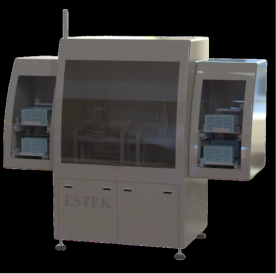
CMOS Imaging Sensor (CIS) Inspection System
CMOS (Complementary Metal Oxide Semiconductor) sensors are semiconductor image sensors that convert light into electrical signals. The applications that use CMOS sensors have dramatically expanded in recent years. Due to their ability to capture sequential images at high frame rates, they are increasingly utilized for industrial inspection, as well as other applications.
ESTEK’s CMOS Imaging Sensor Inspection System is unique. It can define particles on top or underneath of glass or on die.
- POG=Particle on Glass
- POD=Particle on Die
- PUG=Particle under Glass (but not on die, like underside of the glass)
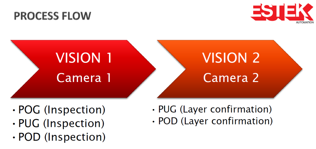
Vision 1: POG/ PUG/POD Camera Configuration
- Vision 1 will perform the inspection and is able to differentiate between (POG) and (PUG/POD) layer.
Vision 2: PUG/POD Camera Configuration
- Vision 2 will then perform the inspection for PUG/POD defects detected by Vision 1 to differentiate between (PUG) and (POD) layer.
Advantages of the ESTEK CMOS Imaging Sensor Inspection System:
- Differentiates POD, PUG & POD defect layer to detect assembly process issues
- Includes Glass, Epoxy, Die, Wire Bond Inspection
- Die Surface Contamination
- High UPH
Two ESTEK Die Sorters Meet Your Needs
The ESTEK Die Sorter comes in two models – Wafer to Wafer Die Sort and Multi-Carrier Die Sort. Both are fully automated, high-speed machines that offer the precision of ESTEK’s superior technologies.
EDS 15 – Wafer to Wafer Die Sort
EDS15 is a fully automated and high-speed die sorter. It can handle any wafer size up to 300mm and can reconstruct wafers to different output form factors. Features include:
- Machine throughput up to 20,000 UPH
- Ability to handle die size of 04×02 mm or larger
- Side Wall Inspection capability with ESTEK’s proprietary special lighting design
This system is used for wafer-to-wafer sorting applications with turret pick and place mechanisms. It offers ultimate performance coupled with versatility. Plus, it is flexible enough to handle the most challenging die sorting applications.
To see this system in action, click here to view a video.
EMS 10 – Multi Carrier Die Sorter
This fully automated and high-speed die sorter can handle any wafer sizes up to 300mm. Configurable for Multi Carrier:
- Wafer Frame 300mm Wafer
- JEDEC Tray
- Waffle/Gel Pack
- Grip Ring
- Tape & Reel
Check out the system video – click here.
We think you will be excited about these innovative systems! If you are looking for superior performance and excellent quality, ESTEK’s systems are a perfect choice.